- 您现在的位置:买卖IC网 > Sheet目录17359 > ADR430ARZ (Analog Devices Inc)IC VREF SERIES PREC 2.048V 8SOIC
ADR430/ADR431/ADR433/ADR434/ADR435/ADR439
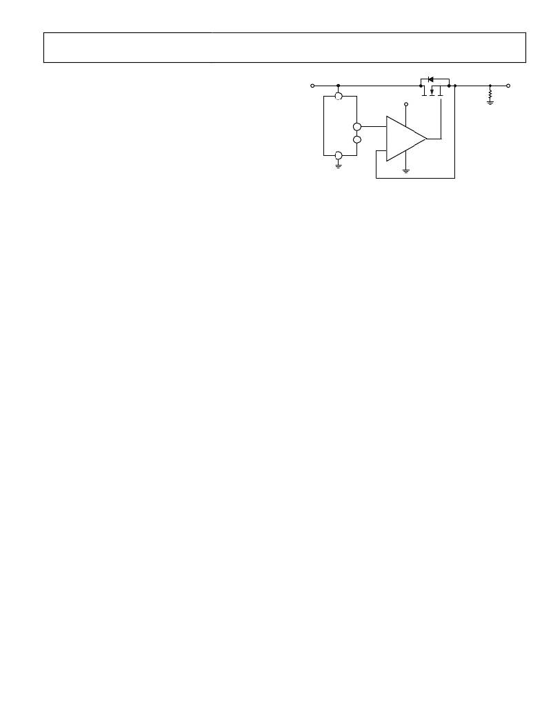
PRECISION BOOSTED OUTPUT REGULATOR
A precision voltage output with boosted current capability can
be realized with the circuit shown in Figure 43. In this circuit,
V IN
2
V IN
5V
N1
R L
25 ?
V O
U2
U2 forces V O to be equal to V REF by regulating the turn-on of
N1. Therefore, the load current is furnished by V IN . In this
configuration, a 50 mA load is achievable at a V IN of 5 V. Moderate
heat is generated on the MOSFET, and higher current can be
achieved with a replacement of the larger device. In addition,
U1
ADR431
V OUT 6
TRIM 5
GND
4
+
–
2N7002
V+
AD8601
V–
for a heavy capacitive load with step input, a buffer can be
added at the output to enhance the transient response.
Rev. J | Page 21 of 24
Figure 43. Precision Boosted Output Regulator
发布紧急采购,3分钟左右您将得到回复。
相关PDF资料
RB-2424S/H
CONV DC/DC 1W 24VIN 24VOUT
A9AAT-1706E
FLEX CABLE - AFH17T/AE17/AFH17T
RBC08DCMS
CONN EDGECARD 16POS .100 WW
ADR443ARMZ
IC VREF SERIES PREC 3V 8-MSOP
HCC05DRXS
CONN EDGECARD 10POS DIP .100 SLD
A9CAG-0403F
FLEX CABLE - AFG04G/AF04/AFE04T
L-07C10NJV6T
CER INDUCTOR 10NH 0402
A9CAA-0308F
FLEX CABLE - AFG03A/AF03/AFE03T
相关代理商/技术参数
ADR430ARZ-REEL7
功能描述:IC VREF SERIES PREC 2.048V 8SOIC RoHS:是 类别:集成电路 (IC) >> PMIC - 电压基准 系列:XFET® 标准包装:2,000 系列:- 基准类型:旁路,可调节,精度 输出电压:1.24 V ~ 16 V 容差:±0.5% 温度系数:- 输入电压:1.24 V ~ 16 V 通道数:1 电流 - 阴极:100µA 电流 - 静态:- 电流 - 输出:20mA 工作温度:-40°C ~ 85°C 安装类型:通孔 封装/外壳:TO-226-3、TO-92-3(TO-226AA)成形引线 供应商设备封装:TO-92-3 包装:带卷 (TR)
ADR430B
制造商:AD 制造商全称:Analog Devices 功能描述:Ultralow Noise XFET Voltage References with Current Sink and Source Capability
ADR430BR
制造商:Rochester Electronics LLC 功能描述: 制造商:Analog Devices 功能描述:
ADR430BR-REEL7
制造商:Analog Devices 功能描述:V-Ref Precision 2.048V 30mA 8-Pin SOIC N T/R
ADR430BRZ
功能描述:IC VREF SERIES PREC 2.048V 8SOIC RoHS:是 类别:集成电路 (IC) >> PMIC - 电压基准 系列:XFET® 标准包装:3,000 系列:- 基准类型:旁路,精度 输出电压:3V 容差:±0.5% 温度系数:100ppm/°C 输入电压:- 通道数:1 电流 - 阴极:82µA 电流 - 静态:- 电流 - 输出:15mA 工作温度:-40°C ~ 85°C 安装类型:表面贴装 封装/外壳:6-TSSOP(5 引线),SC-88A,SOT-353 供应商设备封装:SC-70-5 包装:带卷 (TR) 其它名称:296-20888-2
ADR430BRZ-REEL7
功能描述:IC VREF SERIES PREC 2.048V 8SOIC RoHS:是 类别:集成电路 (IC) >> PMIC - 电压基准 系列:XFET® 标准包装:2,000 系列:- 基准类型:旁路,可调节,精度 输出电压:1.24 V ~ 16 V 容差:±0.5% 温度系数:- 输入电压:1.24 V ~ 16 V 通道数:1 电流 - 阴极:100µA 电流 - 静态:- 电流 - 输出:20mA 工作温度:-40°C ~ 85°C 安装类型:通孔 封装/外壳:TO-226-3、TO-92-3(TO-226AA)成形引线 供应商设备封装:TO-92-3 包装:带卷 (TR)
ADR431
制造商:AD 制造商全称:Analog Devices 功能描述:Ultralow Noise, High Accuracy
ADR431A
制造商:AD 制造商全称:Analog Devices 功能描述:Ultralow Noise XFET Voltage References with Current Sink and Source Capability
